

Knowledge center
PFC has decades of flex circuitry experience across industries. Our Knowledge Center is a resource for the questions that arise when embarking on a new design, considering a flex circuit over other technologies, or are new to flex technology. Our cutting-edge technology and industry leading skills has made PFC the flex circuit experts. Our in depth understanding of the flex industry aids in creating a clear path to successfully launching flex technology for customers.
Design
PFC assisted designs are created for advanced applications and specific requirements. Our designs are RoHS compliant and meet quality standards. PFC Designers improve circuit reliability and functionality. We provide designs and products that meet demands for thinner, lighter and smaller technology.
PFC Quotation Checklist Project Checklist Drawing Notes
Mechanical
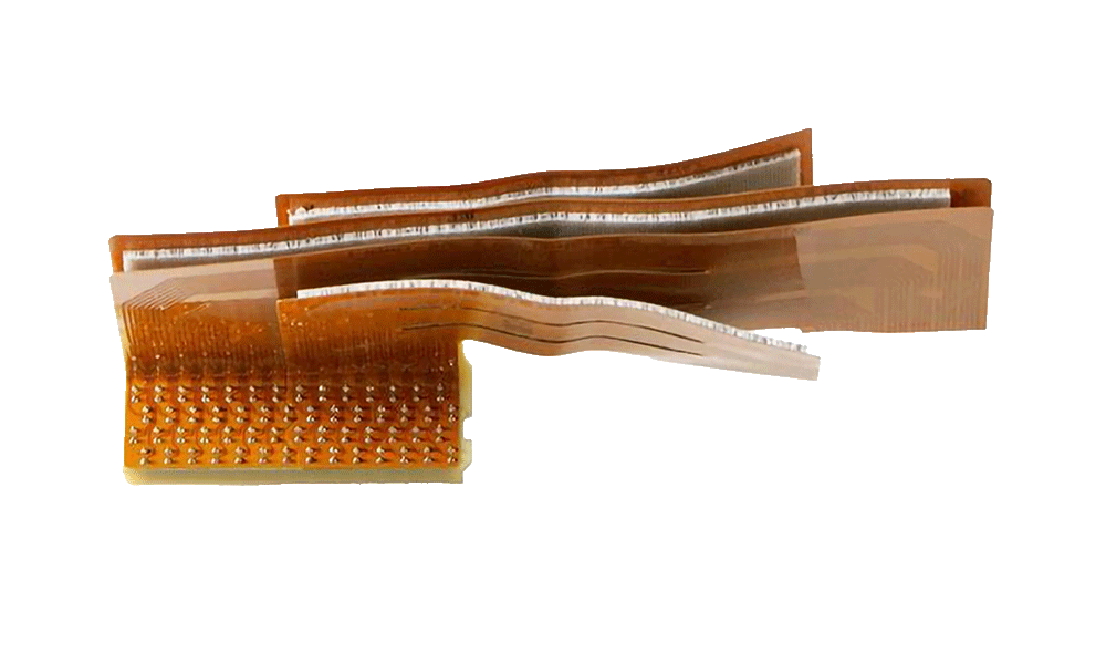
HDI Flex Circuit Technology
PFC’s high density capabilities offer customers a wide variety of custom flexible circuits
with features such as extended lengths, multilayer, non- traditional material
constructions, and specialized foils. The properties of flex-based materials enable
smaller applications with the benefit of reduced weight and optimized packaging
utilization. Our goal is to facilitate new designs that require smaller footprints and ultradense and precise conductor geometries.
PFC Recommended Design Guidelines
Advances in materials and etching technologies have made HDI – high density flex geometries attainable. Standard copper clad-foil for HDI flex circuitry has 18-microns thick copper and, in some cases, thinner. Material choices are a large factor in PFC’s ability to provide cost-effective, high-density circuits.
Our expertise
- HDI flex circuit technology leader for over a decade.
- Experienced builders of production 50-micron trace and space.
- Provider of 37.5-micron trace and space flex circuits in prototype quantities.
- PFC’s technology roadmap is driving flex circuit technology to below 25-micron trace and space.
- PFC’s understanding of key materials, etching processes and design allow PFC to continue to improve on HDI flex circuitry technology.
Micro Vias
High density via fabrication dramatically increases the I/O count. Mechanical drilling of vias is now being done as small as 0.004” (100 micron) diameter. Laser drilling can be done at 0.002” diameter (50 micron) on thin substrates. While PFC offers laser capabilities, the cost to laser each hole one by one becomes expensive.
- Blind and/or buried vias
- Via fill
- Via-in-pad
- 20 µm circuit geometries
- 25 µm dielectric layers
- n50 µm laser via
| DESCRIPTION | HDI FLEX CIRCUIT |
|---|---|
| Lines | 50/50 µm |
| Microvias/pads diameter | 50/200 µm |
| Thinnest copper | 25 µm |
| Thinnest dielectric thickness | 12 µm |
| Conductor width tolerance | +/- 20% |
| Artwork to soldermask tolerance | +/- 25 µm |
| Layer count | 4 |
| DESCRIPTION | ULTRA-HIGH HDI FLEX CIRCUIT |
|---|---|
| Lines | 37.5/37.5 µm |
| Microvias/pads diameter | 40/100 µm |
| Thinnest copper | 9 µm |
| Thinnest dielectric thickness | 12 µm |
| Conductor width tolerance | +/- 15% |
| Artwork to soldermask tolerance | +/- 25 µm |
| Layer count | 8 |
Materials and Surface Finishes
Materials & Surface Finishes
Stiffeners are materials added to a flex circuit to rigidize areas. Rigidizing is recommended under SMT components, but not required. Other areas to consider rigidizing include:
- Hole patterns stiffener image
- Forcing bends
- Increasing overall thickness
- Protecting solder joints
- Die attach platform for wire bond components
- Heat dissipation
Types of Stiffener Materials
FR4/G10 Stiffeners
- Bonded with PSA or thermal-set adhesive.
- Adds rigidity to connector area or used as carrier panel.
Polyimide Stiffeners
- Bonded with PSA or thermal-set adhesive.
- Used to add thickness or add strength in high wear areas.
Other Materials
- Stainless Steel
- Aluminum
- Ceramic
Placing Stiffener
Stiffener and coverlay termination points should overlap a minimum of .030” to avoid stress points. placing stiffener PFC can assist with the location of stiffeners, identification of the material and the required thicknesses.
Standard Flex Circuit Finishes
- Hot air solder level
- Immersion gold over electroless nickel (enig)
- Immersion tin (white tin)
- Electroplated soft or hard gold over electroplated nickel (both phosphorus and low sulfamate)
- OSP (Organic Solderability Preservative) limited use
RoHS Compliancy
- Bare flex circuits are RoHS compliant if they have a RoHS compliant surface finish.
- A common problem with RoHS circuits is via reliability.
- The different CTE’s (coefficient of thermal expansion) in the materials must be matched more closely in high end designs.
Mechanical
Flex circuit design must consider the mechanical characteristics of bending and potentially cycling the circuit. Other mechanical aspects that affect a flex circuit are size, shape, thermal properties, and mechanical stability in key areas. Additional factors are reliability & stiffeners, and materials. Below are general guidelines for static and dynamic circuits:
Static (One-time Bend)
- Bend radius for flex to install is 10x the thickness of the flex this can often be pushed to 5x.
- Can use stiffeners to create a natural folding configuration
- Keep stress concentrators well away from bend areas
- A soft adhesive system may “pucker” on the inside of a tight bend radius
Dynamic (Multiple Bends)
- Best practice- bend radius for dynamic flex is 100x the flex thickness
- Conductor thickness and width should remain constant in bending areas
- Conductors should be staggered from layer to layer and not stacked on top of each other to increase flexibility
- Conductor thickness and width should remain constant in bending areas
Reliability and Bendability
Flex Circuit Reliability/Bendability
“How much can a flex circuit bend?” This is the most frequent question we hear. The standard IPC answer is 10 times the thickness of the material. Section IPC-2223 offers reasonable information on bend radius calculations. PFC considers various factors when designing a flex circuit for high reliability.
- Grain direction in the copper is important for tight bend radii
- The stiffness of a flex is primarily driven by the copper weight
- Kapton thickness is critical
- Bend location
- Flex circuit application reliability
Reducing Overall Thickness in the Flex Area
- Reduce the base copper weight (and the corresponding adhesive thicknesses) or reduce the dielectric thickness.
- Use non-adhesive base materials, which typically reduce the starting thickness of each substrate by 12-25um (0.0005”- 0.0010”) when compared to adhesive based substrates.
- Eliminate copper plating on the conductors in the flexing area (dynamic region) by utilizing selective (pads plating/button plating-only) allowing the circuit to have increased flexibility.
Making a Strong Flex Circuit
Conductors should be staggered from layer to
layer and not stacked on top of each other to
increase flexibility.
- Conductor thickness and width should remain constant in bending areas.
- Balance the conductor weights and material thicknesses on each side of the neutral bend axis.
- Bend radius of a flex should be approximately 10 times the material thickness and at least 500um (0.020”) away from the plated through hole.
- Incorporate tear stops or reliefs for slits in the circuit. The end of the slit represents a vulnerable point for a tear to start and to propagate.
Zif Designs
ZIF connectors are a reliable low-cost interconnect solution. While it simplifies assemblies, detailed planning is important to designing the ZIF interface for a flex circuit. Every ZIF connector manufacturer will call out different dimensional requirements. Connector specifications will be needed for a quotation.
ZIF Design (Zero Insertion Force Interface)
- Ecobond or fillet transition areas from a rigid area to the flex
- Make sure drawings/files clearly show what is top and bottom
- Zif end traces should be pulled back 0.25 mm. from the outline to avoid damage during die cutting.
Exceptions:
- Electroplated gold unless it is built with no outside connections
- Rigid flex due to electrical test considerations
Coverlay
- Coverlay openings need to be a minimum of 0.25 mm. larger than the through hole. This is not acceptable for class 3 products
- The web between two coverlay openings should be at least 0.25 mm. To provide adequate adhesion
- Do not have any coverlay opening line up to the stiffener below
- It is much more difficult to register a soldermask- try to design to .075 -0.1.mm minimum space mask edge to feature and minimum solder mask width of 0.1mm.
- For a coverlay increase the above by a factor of 2
Electrical
Electrical factors are considered when designing and producing flex circuits to ensure flex circuit electrical and mechanical aspects work cohesively. During our electrical analysis, we will find the best options for the impedance, shielding, bendability, and material. PFC provides an unmatched electrical solutions for flexible circuits.
- Thickness & weight
- Gig/sec speeds
- Spacing & tempurature
- Electrical properties
- Characteristics impedance
- High current / high power interconnects
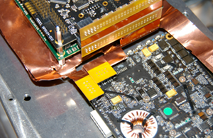
High Current Flex Circuit Designs
Flex circuits are regularly used in high current/power applications. Some application examples of designs produced at PFC include bus bars, backplanes, and power distribution cables. Most of the high current applications PFC develops are to replace wire harnesses
The benefit of using flex circuit replacing a wire harness includes:
- Decreased assembly time
- Reduced materials and part numbers
- Increased reliability – reduction of assembly errors
- Decreased space, increased air flow
- Improved thermal characteristics
- Increase interconnect options
IPC 2152
IPC has come out with a new specification on current carrying capabilities for PCBs and
flex circuits in 2010: IPC 2152. This new specification takes the place of IPC 2221 which
was developed in 1955!
Copper Thickness
The thicker the copper, the more current a flex circuit can carry. PFC has the ability to provide flex circuits utilizing up to 560-micron thick copper for power applications. Available copper
weights for power applications in microns include:
IPC 2152 contains information that can be used to develop current-carrying capacity
guidelines for individual designs. Through the use of computer modeling and
information within IPC 2152 and its appendix, current carrying capacity design
guidelines can be optimized for any variation in printed circuit technology. Until the
publication of IPC 2152, this was not possible with the available public information
If you are designing a high current flex, PFC urges you to obtain IPC 2152. You can
purchase the publication from the IPC online store.
TEMPERATURE RISE AND MATERIAL CTES (THERMAL EXPANSION)
The biggest design consideration for high current flex circuit applications is temperature
rise and material thermal expansion. Below is a list of relevant material expansion
characteristics.
- Copper 18 ppm/deg C
- Polyimide 25 ppm/ deg C (x,y) and 100 ppm/ deg C (z)
- Acrylic adhesive (deg C (x,y,z)
- Acrylic adhesive (>tg 40C) – 400 ppm/ deg C (x,y,z)
- Polyimide adhesive (deg C (x,y)
| MICRONS | OUNCES |
|---|---|
| 70 | 2oz |
| 105 | 3oz. |
| 140 | 4oz. |
| 175 | 5oz. |
| 245 | 7oz. |
| 420 | 12oz. |
| 560 | 16oz. |
Impedance control
Electrical Impedance Control
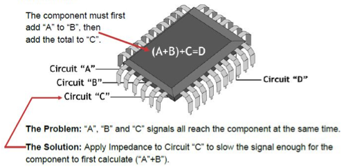
This is the measure of opposition to time-varying electric current in an electric circuit. Simply put, impedance control is the slowing down of an electrical circuit. As flex circuit design and components become more complicated, smaller and faster, it becomes necessary to slow certain circuits down, allowing specific functions of components to perform before others. The increase in processor clock speed and component switching speed on modern flex circuit means that the interconnecting paths (traces) can no longer be regarded as simple conductors.
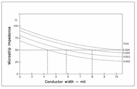
Design Factors Affecting Flexible Circuit Impedance Control
- Impedance (Zo) is measured in Ohms (Ω) and should not be confused with resistance – you cannot measure impedance with an ohmmeter
- Target impedance is usually between 25Ω, and 125Ω
- Typical result of a 75Ω controlled impedance on a 0.007” trace is a signal slowdown of approximately 166ps/in
- Conductor width increase, impedance decreases
- Copper thickness (weight) increase, impedance decreases
- Laminate thickness increase, impedance increases
- Dielectric constant increase, impedance decreases
- Inductance increase, impedance increases
- Capacitance increase, impedance decreases
Physical Factors Affect Flexible Circuit Impedance Control
Physical characteristics of impedance trace:
- Height of trace (T1)
- Width of trace at top (W2)
- Width of trace at bottom (W1)
- Distance to other copper features (H1)
- Dielectric constant of PCB material (Er)
- SIMPLE IMPEDANCE MODELS
Complicated Impedance Models
Some PCBs may have multiple impedance requirements! More impedance
requirements mean more impedance coupons, which can decrease the amount of
usable panel space for PCBs.
Flexible Design Considerations: Impedance & Capacity Control
Double-layer and multi-layer flexible circuits are ideally suited for providing interconnections that are specifically designed to provide desired levels of signal integrity. Construction techniques commonly referred to as “stripline” or “microstrip” are particularly well suitedfor these applications.
Microstrip
- Typically a 2 layer flex – 1 signal, 1 groundMicrostrip and impedance and capacitance control
- Generally used in lower frequency applications less than 500MHz signal speeds; where crosstalk is a concern, should have a reference plane; microstrip construction are flexible enough for dynamic applications.
- Benefits: More flexible, better for power lines and typically less expensive
Stripline
- Typically a 3 layer flex – 1 signal and 2 groundStripline and impedance and capacitance control
- Generally used in higher frequency applications >500MHz because of crosstalk concerns; mostly used for less dynamic or static applications
- Benefits: Better signal integrity characteristics (cleaner signals)
- Cons: More expensive and less flexible
Relationships within a Controlled Impedance Microstrip Design
Shielding
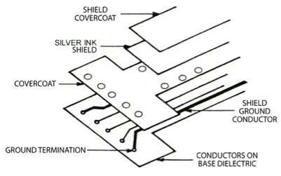
Applications with limitations to the electromagnetic and/or electrostatic interface may require shielding. This can be accomplished through multiple methods. Shields are designed and used for EMI and ESD considerations as well as impedance requirements. Shielding provides various advantages to a flex circuit.
PFC recommends 4 types of shielding:
- Copper clad
- Copper cross hatch
- Silver paste/epoxy
- EMI Thermoplastic shielding film
Copper has the best shielding characteristics. Silver allows more flexibility and at a slightly lower cost. Shielding film is most flexible but a higher cost solution.
Example of conductor Ink (silver) shielding
Flexibility
- Semi-flexible
- Flexible
- Flexible
- Most flexible
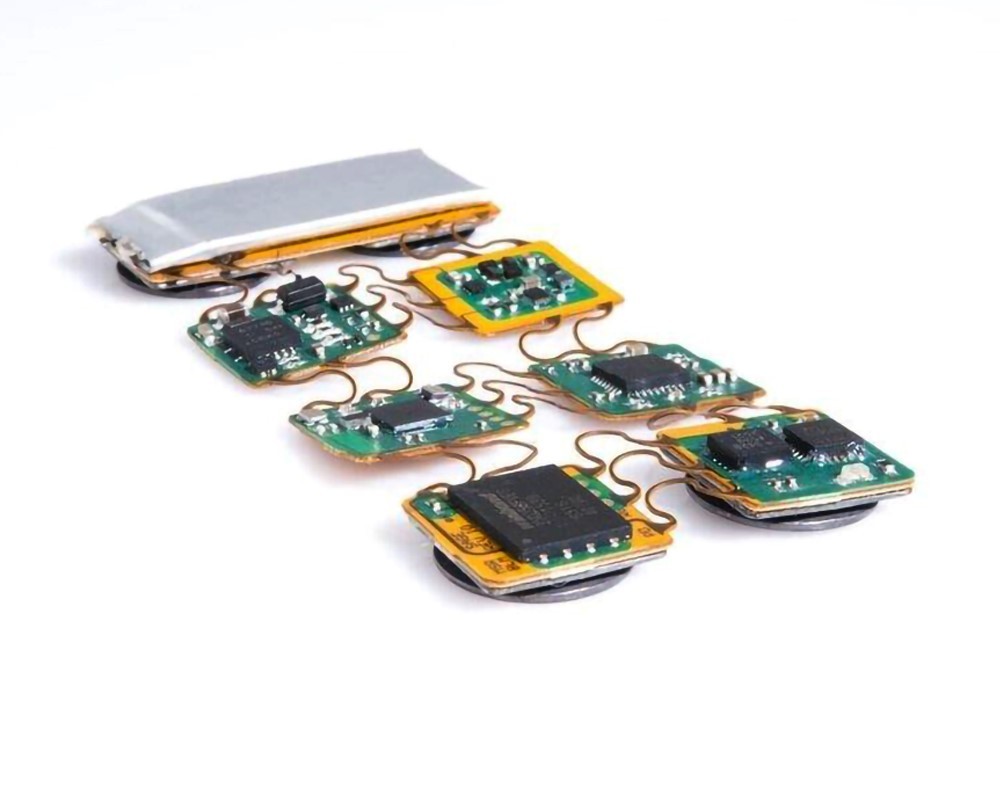
Flex Circuit Materials
Our flex experts offer a vast knowledge of flex circuit materials. We provide a Materials Stack Up list of specific materials and thicknesses that will be used in the manufacturing of your circuit. This will include required adhesives, stiffeners and any special drilling requirements such as blind and buried vias.
| Materials | PFC Approved |
|---|---|
| Insulating Materials | Polyimide |
| Adhesiveless Materials | DuPont APPanasonicEspanex |
| Coverfilm/ Covercoat/ Coverlay | Kapton (Pyralux), Espanex, DuPont-Black, Taiflex-Black&White |
| High Speed Laminates | TK- DuPointTaconic |
| Flexible Solder Mask | Various per IPC-840 Class 3 |
| Rigid Solder Mask | Taiyo PSR |
| Metals | Copper 9-750 micron (.0008 - .030) thickBeryllium CoppyNickel Alloys |
| Finishes | Immersion gold over Electroless nickel Immersion TinHot air solder level (tin-lead)Hard goldSoft goldOSP (Organic Solderability Preservative) |
| Shielding Materials | Copper Silver paste/inkTatsuta |
| Stiffeners | PolyimideMachined Metal, Aluminum (cast)CeramicFR-4Black FR-4 |
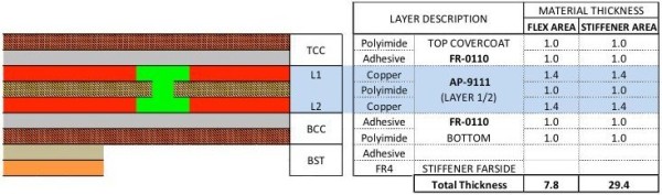
Material Stack Up
Material Stack-Up
After a thorough analysis of the project, PFC will provide a list of specific materials and thicknesses that will be used in the manufacturing of the circuit. This will include: required adhesives, stiffeners and any special drilling requirements such as blind and buried vias.
Example Stack Up
UL Constructions
Electronic equipment, in many cases, require a UL (Underwriters Laboratory) certification. In turn, the components that make up the electronic system must be certified, including flex circuits.
UL does not require the flex circuit itself to be approved or certified. However, it must be manufactured using UL approved flexible circuit material and manufacturing processes. In order to get an approval from UL, PFC provides UL with documentation and samples of a specific construction
UL will test and approve that specific construction. Once the construction is approved, PFC can use that specific construction on other circuits as UL approved construction.
PFC offers a full range of UL approved Dupont materials, including AP and FR laminates, coverlays, and a full range of Panasonic and Espanex materials. Additionally, PFC just had the full line of Taiyo “BN” soldermasks recognized for any color.
Visit the UL website for many of the approved constructions for PFC and more information on UL approved flexible circuit material.